Lab 3 - Due 10/31 - 11:59PM on UBLearns
Lab 3: Transistor Sizing
Size all the transistors from Lab 2: Part I (CMOS Full Adder) for
- Performance
- Symmetric rise & fall times
Report your observations (Propagation Delays, Rise/Fall times, Power Consumption) with supporting extracted view simulation results.
Submit a PDF on UBLearns with your findings.
Lab 2 - Due 10/07 in Lab
Lab 2: Full Adder & Transmission Gate (Due: 10/21, 10/22 at beginning of Lab)
Part I: Implement a full adder at the transistor level (CMOS).
See slide 58 of Lecture 3-4 CMOS Devices & Logic
Part II: Implement Transmission Gate Logic (TGL) of Full Adder.
See slide 77 of Lecture 3-4 CMOS Devices & Logic
- Create symbol for transmission gate (slide 40).
- Maybe a simulation is a good idea?
- Compare this full adder from the one in Part I.
- Which has less power? By how much?
- Which is faster? How much (propagation delay)?
Part III: Implement Transmission Gate 2-to-1 Mux.
See slide 75 of Lecture 3-4 CMOS Devices & Logic
For all parts make sure you have the following:
- Schematic
- Simulation (have sufficient test cases)
- Symbols
- Layout
- DRC & LVS pass
Lab 1 - Due 09/23 in Lab
Lab 1: Getting Started with
Cadence Virtuoso - Implementation of Basic Logic Gates (Due: 9/30, 10/1 in Lab)
What
you can do before coming to the lab:
1. It is highly recommended that you go over the
Cadence Virtuoso setup and tutorial pages
as you work on this assignment to correctly setup your tool and access. Follow
all steps given under Cadence Virtuoso setup. The documentation provided under
the help menu in each cadence tool also contains detailed information on using
the tools.
2. Go through the lecture that has
covered the design of Complementary CMOS circuits and work on designing
the circuit. This saves you time during the lab session and you have more time
to work on your cadence implementation.
Part-I: CMOS Inverter
Design
Design a CMOS inverter in Cadence. The width
of the PMOS should be 240nm and NMOS transistors
should be 120nm. Their lengths can both be
set to 45nm.
For simulations,
set the inverter input signal to have a rise time of 0.5ns, fall time of 0.5ns,
pulse width of 2ns, period of 5ns. Use model file: /util-cse/cadence/local/gpdk045_v_6_0/gpdk045/../models/spectre/gpdk045.scs
1.
Create the inverter schematic using Virtuoso
Schematic XL
2.
Simulate the inverter using spectre simulator in the Analog Design
Environment (ADE) Explorer tool. Measure the propagation delay of the inverter
in the waveform window
3.
Create an inverter symbol using Virtuoso
Symbol L
4.
Layout the inverter in Virtuoso Layout XL.
5.
Pass DRC & LVS checks
6.
Extract the layout and simulate the extracted
version.
7.
Measure the propagation delay of the inverter
in the waveform window
8.
Is there a difference in the propagation
delays between the circuit schematic and extracted layout? Why/Why not?
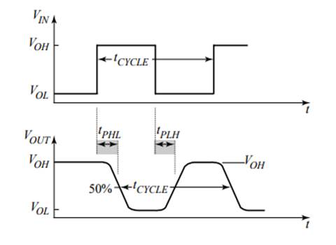
Propagation Delay (tp): Propagation delay
expresses the delay experienced by a signal when passing through a gate. tpLH defines the response time of the gate
for a low to high output transition, while tpHL refers
to a high to low transition. The overall propagation delay is conservatively
defined as the average of the two delays tpLH and tpHL.
Part-II: Basic Logic Gates
You
will have to implement the schematic and layout for basic 2-input gates
i. NAND
ii. NOR
iii. XOR
Create
symbols for each schematic.
Useful
tips:
1.
Another important thing to note is to keep the width of the PMOS
transistors double the width of the NMOS transistors. The width of the NMOS and PMOS transistors should be 120nm and 240nm, respectively. Their
lengths can both be set to 45nm.
2.
As you have to
design 2-input gates, you should test your circuit for all possible combination of inputs. This can be done using two pulse
inputs, one with twice the time period of the other.
Another effective method to give stimuli is using bit inputs with 0.01ns rise
and fall times.